USB is a Universal Serial Bus interface standard used to connect computers and external devices, enabling them to perform data transfer and communication. The USB standard was designed to simplify the connection between computers and peripheral devices. It has become very popular due to its compatibility with multiple platforms and operating systems, low-cost implementation, and ease of use. Most computers today are equipped with several USB ports, and USB has become the interface of choice for most home and office peripherals, including printers, cameras, modems, and portable storage devices.
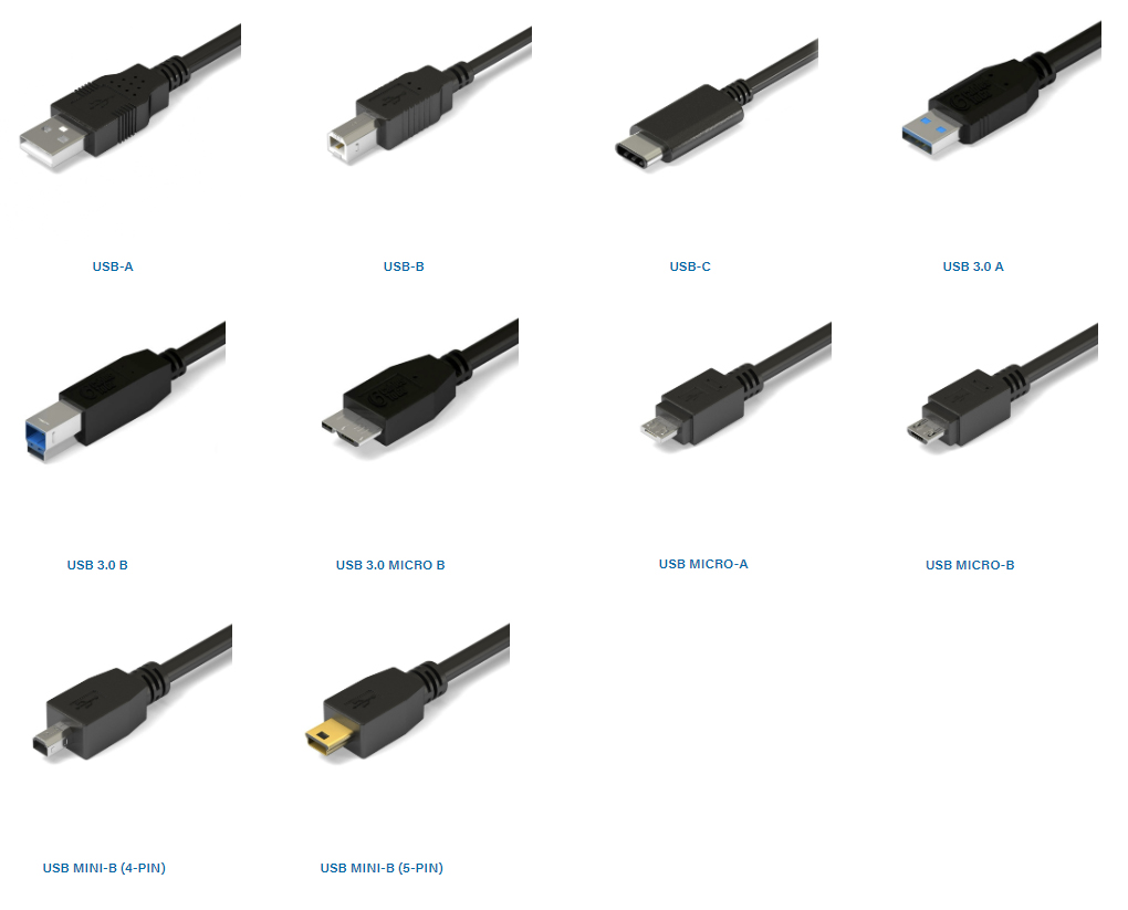
With the passage of time, the USB interface standard has experienced USB1.0, USB2.0, USB3.0 and USB4.0. Each generation of USB interface is subdivided into USB Type A/B/C/Mini according to the characteristics of the supported devices.
Layout Requirements of PCB for USB Interface
- The USB interface should be positioned close to the edge of the board or the structure positioning, and protrude out of the edge of the board to a certain position (except direct plug-in), for easy plugging and unplugging.
- ESD and common-mode inductors should be placed close to the USB interface, and the order of placement is ESD-common-mode inductor-RC.
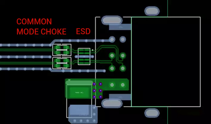
- There must be a certain distance between ESD and USB, and the situation of post-soldering needs to be considered.
- When laying out, try to keep the differential lines as short as possible to shorten the distance between differential lines.
Wiring Requirements of PCB for USB Interface
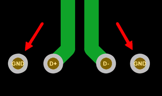
- USB should be differential. Impedance control is 90 ohms and includes ground processing. The total length should not exceed 1800mil.
- Shorten the trace length as much as possible, and give priority to the wiring of high-speed USB differential (RX, TX differential). When routing USB differential traces, try to reduce layer-changing vias as much as possible, so as to better achieve Impedance control to avoid signal reflection.
- Vias will cause discontinuity in trace impedance. Add a pair of return ground vias at the place where each via is punched and changed layers for signal return and layer change.
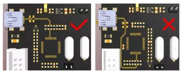
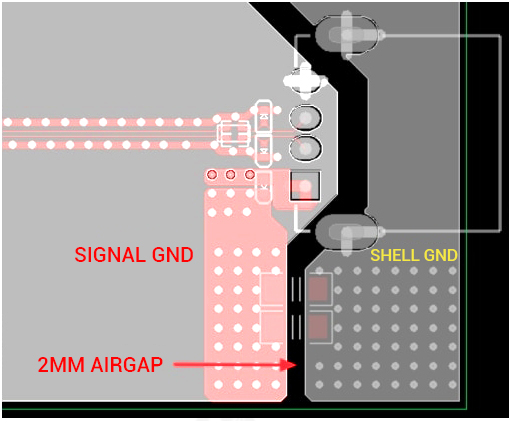
- The USB connectors have locating posts on both sides, which are connected to the protective ground. When separating them, it is necessary to ensure a 2mm distance from GND and to create multiple holes in the protective ground area to ensure a secure connection, as shown in the diagram below.
- Due to factors such as pin distribution, vias, and routing space, there is a tendency for the lengths of differential lines to not match. Once the wiring lengths do not match, it can lead to timing deviations and common-mode interference, which will reduce signal quality. Therefore, it is necessary to compensate for the mismatch in the case of differential pairs, ensuring that the line lengths match, with a typical length difference controlled within 5 mils, following the guidelines for ensuring equal-length differentials.
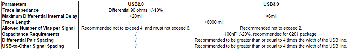
The Comparison of PCB Layout Requirements Between USB2.0 and USB3.0
PCB Design for Type C Interface
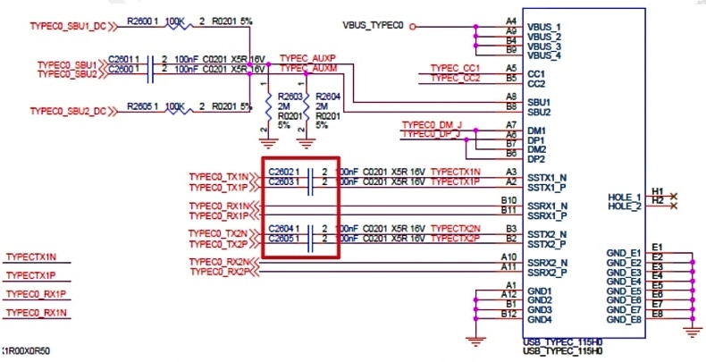
USB Type C, also known as USB-C, should be noted as just a type of interface and is not related to the version of USB. The highlight of this interface lies in its thinner design and faster transfer speeds. One of the key features of the Type-C reversible plug is its support for plugging in from either side, primarily aimed at thinner and sleeker devices. The diagram below shows the pinout definition for the Type-C interface.
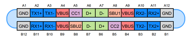
For USB Type C Receptacle
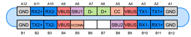
For USB Type C Plug
PCB design requirements for Type C interface:
- ESD, common mode inductors, and capacitors should be placed near the Type C interface in the following order: ESD -> Common Mode Inductor -> Capacitor. It's also important to ensure a certain distance between ESD and the Type C interface, taking into account post-soldering conditions.
- The coupling capacitors for the TX signal lines should be placed near the interface, while the coupling capacitors for the RX signal lines are provided by the device end, as shown in the diagram below.
- Maintain an impedance of 90 ohms ±10% for Type C differential traces. To ensure impedance continuity, there should be a solid reference plane without splits, and the number of signal vias when transitioning layers should not exceed 2.
- For Type-C, there are four sets of differential signals: (TX1+, TX1-), (RX1+, RX1-), (TX2+, TX2-), and (RX2+, RX2-), along with two sets of D+/D- differential signals, making a total of six pairs of differential lines. The requirement for the differential signal lines is to be adjacent to at least one ground plane, and it is preferable to have ground planes on both sides. Routing should be as short as possible, with a maximum length not exceeding 6000 mil.
- Ensure equal length matching for Type-C differential lines and an internal length mismatch of less than 6 mil. Compensation should be performed in accordance with the differential length matching specifications.
- Ensure that the impact of Type C differential pairs on adjacent pairs or other signals is minimized. It is recommended to have a spacing of greater than or equal to 4 times the Type C trace width between Type C differential pairs. Maintain spacing between Type C differential pairs and other signals as large as possible, preferably greater than or equal to 4 times the Type C trace width.
- CC1/CC2 are two critical pins with various functions, including connection detection, distinguishing between the front and reverse sides, distinguishing between DFP and UFP, i.e., configuring Vbus for host and peripheral roles. When routing, it's important to ensure these traces are appropriately thickened.
Note: When the Type-C connector operates at a speed of ≥8Gbps, please follow the following design requirements.
When routing within the connector, the traces should exit from the center. If at one end of the connector, high-speed signals do not have a GND pin adjacent to them, it is advisable to add a GND via next to them during the design.
If the interface's signal operates at a speed ≥8Gbps, the connectors for these interfaces should meet the relevant standard requirements (such as HDMI 2.1/DP 1.4/PCI-E 3.0 protocol standards). It is recommended to use connectors from manufacturers such as Molex, Amphenol, HRS, and others.
Depending on the interface selection, either one layer or two layers of ground plane can be excavated. If the ground reference layer beneath the connector pads on L2 is excavated, a separate reference plane on L3 should be designated as the ground reference. If both the ground reference layers on L2 and L3 are excavated, then L4 should be designated as the ground plane and serve as a separate reference plane. The size of the cutout should be determined based on the connector model and verified through simulation in consideration of the actual stack-up.
It is recommended to place two ground vias for each ground pad of the connector, and these ground vias should be positioned as close to the pad as possible.


