PCB Prototype the Easy Way

Full feature custom PCB prototype service.

Help Center
Sending a message
9:00 - 23:00, Mon.- Sun. (GMT+8)
Service hotlines
+86 571 8531 7532

9:00 - 18:00, Mon.- Fri. (GMT+8)

9:00 - 12:00, Sat. (GMT+8)

(Except Chinese public holidays)

Advanced High-quality PCB Capabilities

Advanced PCB Manufacturing Capability,The information below details some of the key capabilities that PCBWay can offer and support today.

When you order advanced PCBs from the PCBWay, you are buying quality that pays for itself over time.

At first sight, PCBs differ little in appearance, irrespective of their inherent quality. It is under the surface that we focus on the differences so critical to the PCBs’ durability and functionality. Customers cannot always see the difference, but they can rest assured that PCBWay puts a great deal of effort into ensuring that in turn, their customers are also supplied with PCBs that meet the most stringent quality standards.Highly Specialized Precision PCBs, & Large Scale Production (No order is too small or too large).our customers achieve the best possible time to market and competitive advantage by producing printed circuit boards in a sustainable way at the lowest total cost through our competence, delivery accuracy and product quality.If you want to see standard PCB or quickturn pcb Capabilities, pls click this link. Advanced PCB Manufacturing Capability,The information below details some of the key capabilities that PCBWay can offer and support today.


Advanced PCB Manufacturing Technical Roadmap

Items 2016 2017 2018
Number of Layers General PCB board 2-36 2-40 2-64
Buried IC no yes yes
HDI(buried and blind vias) HDI(2+N+2)
staggered and stacked vias
HDI(4+N+4)
staggered and stacked vias
HDI(7+N+7)
staggered and stacked vias
Materials FR4(shengyi) yes yes yes
High Tg Tg-170 Tg-210 Tg-220
EHalongen Free yes yes yes
High Frequency yes yes yes
Maximum board size 20*30inch(508*762mm) 20*30inch(508*762mm) 20*35inch(508*889mm)
Board thickness 0.21-6.0mm 0.21-6.0mm 0.21-6.0mm
Minimum track line 3mil-inner 3mil-outer 2mil-inner 3mil-outer Portion 2mil-inner 2mil-outer
Minimum Spacing line 3mil-inner 3mil-outer 2mil-inner 3mil-outer Portion 2mil-inner 2mil-outer
Outer layer copper thickness 5oz 7oz 8oz
Inner layer copper thickness 5oz 7oz 8oz
Min. finished hole size(Mechanical) 0.15mm yes yes yes
Min. finished hole size(laser hole) 0.076mm yes yes yes
Aspect ratio 12:1 12:1 12:1
Solder Mask Types and brand NAYA(LP_4G) yes yes yes
Tamura(TT19G) yes yes yes
TAIYO(PSR2200) yes yes yes
Solder Mask Color green;blue;red;white;black yes yes yes
Impedance Control Tolerance ±10%,50Ω and below:±5Ω yes yes yes
Plug via hole Min.size can be plugged: 0.15mm(CNC)|0.1mm(Laser Blind/buried vias) 0.15mm(CNC)|0.1mm(Laser Blind/buried vias) 0.15mm(CNC)|0.1mm(Laser Blind/buried vias)
Max.size can be plugged: 0.7mm 0.7mm 0.7mm
Min. annular ring can be kept 3mil 3mil 3mil
Min. distance between the IC pads
can keep SM bridge
8mil 8mil 8mil
Min. SM bridge for green soldermask 3mil 3mil 3mil
Min. SM bridge for black soldermask 4mil 4mil 4mil
Surface Treatment HASL yes yes yes
ENIG yes yes yes
OSP yes yes yes
LEAD FREE HASL yes yes yes
GOLD PLATING yes yes yes
IMMERSION Ag yes yes yes
IMMERSION Sn yes yes yes
V-Cut CNC V-cut, degree 20\30\45\60 20\30\45\60 20\30\45\60
V-cut by hand, degree 20\30\45\60 20\30\45\60 20\30\45\60
Outline Profile CNC CNC CNC
Chamfer The angle typeof the chamfer: 20\30\45 20\30\45 20\30\45
Min. distance of jumping chamfer: 5mm 5mm 5mm
Tolerance of the dimension size ±0.1mm ±0.1mm ±0.1mm
Tolerance of the board thickness 0.21-1.0 ±0.1 ±0.1 ±0.1
1.0-2.5 ±7% ±7% ±7%
2.5-6.3 ±6% ±6% ±6%
Tolerance of the finished hole size 0-0.3mm ±0.08mm ±0.08mm ±0.08mm
0.31-0.8mm ±0.08mm ±0.08mm ±0.08mm
0.81-1.60mm ±0.05mm ±0.05mm ±0.05mm
1.61-2.49mm ±0.075mm ±0.075mm ±0.075mm
2.5-6.0mm +0.15/-0mm +0.15/-0mm +0.15/-1mm
>6.0mm +0.3/-0mm +0.3/-0mm +0.3/-1mm
Certificates(copies are needed) UL yes yes yes
ISO9001 yes yes yes
ISO14000 yes yes yes
ROHS yes yes yes
TS16949 yes yes yes

Advanced High-quality PCB Manufacturing Capabilities

No. Item Process capability parameter
1 Base material FR-4|High Tg|Halogen-free|PTFE|Ceramic PCB (Scrap rate is too high)|Polyimide
2 PCB type PCB|FPC|R-FPC|HDI
3 Max layer count 64 layers
4 Min base copper thickness 1/3 OZ (12um)
5 Max finished copper thickness 8 OZ
6 Min trace width/spacing Inner layer 2/2mil (H/H OZ base copper)only part trace with this width and space but not all the board with this trace width and space
7 Outer layer 2/2mil (1/3 OZ base copper)only part trace with this width and space but not all the board with this trace width and space
8 Min spacing between hole to inner layer conductor 6mil
9 Min spacing between hole to outer layer conductor 6mil
10 Min annular ring for via 3mil
11 Min annular ring for component hole 5mil
12 Min BGA diameter 8mil
13 Min BGA pitch 0.4mm
14 Min hole size 0.15mm(CNC)|0.1mm(Laser Blind/buried vias)
15 Max aspect ratios 20:1
16 Min soldermask bridge width 3mil
17 Soldermask/circuit processing method Film|LDI
18 Min thickness for insulating layer 2mil
19 HDI & special type PCB HDI(1-7 steps)|R-FPC(2-16 layers)|High frequency mix-pressing(2-20 layers)|Buried capacitance & resistance ……
20 Surface Finish type ENIG|HAL|HAL lead free|OSP|Immersion Sn|Immersion silver|Plating hard gold|Plating silver
21 Max PCB size 609*889mm

Advanced PCB High Performance Materials

Items 
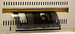
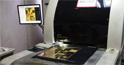
PCB Prototype capacity (area < 1m2;) 
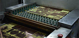
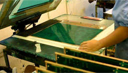
Small and medium batch (area > 1m2)
Materials General Tg FR4: shengyi S1141,Kingboard KB6160A shengyi S1141
High-Tg Halogen-free: shengyi    S1170G Halogen-free TG170,TU-862 HF TG170  shengyi    S1170G Halogen-free TG170 ,TU-862 HF TG170 
Medium Tg Halogen-free: shengyi    S1150G Halogen-free TG150 shengyi    S1150G Halogen-free TG150
High Halogen-free CTI: shengyi    S1151G( CTI&ge;600V) shengyi    S1151G( CTI&ge;600V)
High CTI: shengyi S1600( CTI&ge;600V)Kingboard KB6160C shengyi S1600( CTI&ge;600V)Kingboard KB6160C
Special Material(High low temperature): shengyi    SH260 shengyi    SH260  
High Tg FR4: S1000-2, S1000-2M,IT180A S1000-2, S1000-2M,IT180A
Ceramic powder filled high frequency Rogers4003, Rogers4350, Arlon25N,shengyi S7136 Rogers4350, Rogers4003,shengyi S7136
PTFE high frequency material: Rogers, Taconic, Arlon,Taizhou wangling Rogers, Taconic, Arlon,Taizhou wangling
High Frequency PCB PP RO4450    0.1mm,shengyi    Synamic6, RO4450    0.1mm,shengyi s6
High Speed( 1-5G) MEG4,Tu-862,Tu-662, Tu-768, S7038, S1165, Isola-FR408HR, Isola-FR406,EMC TW -EM370,EM828G IT170GRANP175FM(Nanya) MEG4, Tu-862, Tu-662, Tu-768,S7038, S1165, Isola-FR408HR, Isola-FR406,EMC TW -EM370, EM828GIT170GRA,NP175FM(Nanya)
High Speed( 5-10G) MEG4,Tu-872, N4000-13, M4, Tu-863(Halogen-free),Synamic4, EM-888, I-Speed(Isola) N4800-20SI(Nelco) IT-958G MEG4,Tu-872, N4000-13, M4, Tu-863(Halogen-free), Synamic4, EM-888, I-Speed(Isola) N4800-20SI(Nelco)    IT-958G
High Speed( 10-25G) MEG6, Tu-883,shengyi Synamic6, Meteorwave1000/2000/3000(Nelco), EM-891(EMC TW),EM-888K, IT-968, I-Tera MT40(Isola) MEG6, Tu-883,shengyi Synamic6, Meteorwave1000/2000/3000(Nelco), EM-891(EMC TW), EM-888K, IT-968 I-Tera MT40(Isola)
High Speed(>25G) MEG7, Tu-933,Meteorwave4000( Nelco), IT-988, Tachyon 100G(Isola) MEG7, Tu-933,Meteorwave4000( Nelco), IT-988 Tachyon 100G(Isola)
High Frequency PCB DK 2.2-2.25 RO5880, TLY-5(Taconic) SCGA-500    GF220(shengyi), F4BK225 /
High Frequency PCB DK 2.33 RO5870, TLY-3(Taconic) /
High Frequency PCB DK 2.45 TLX-0(Taconic), TLT-0(Taconic) /
High Frequency PCB DK 2.5-2.55 AD250(Arlon), TLT-9(Taconic), TLY-9(Taconic); SCGA-500 GF255(shengyi), TLT-8(Taconic), TLY-8(Taconic), F4B255 /
High Frequency PCB DK 2.6-2.65 TLT-7(Taconic), TLY-7(Taconic); TLT-6(Taconic), TLY-6(Taconic), SCGA-500 GF265(shengyi), F4B265 /
High Frequency PCB DK 2.7-2.75 AD270(Arlon); TLC-27(Taconic) /
High Frequency PCB DK 2.92-2.94 RO6002, CLTE( Arlon) /
High Frequency PCB DK 2.95 AD295(Arlon), TLE-95(Taconic) /
High Frequency PCB DK 3.0 SCGA-500    GF300(AR-320(Arlon), (Taconic), TLC-30(Taconic), RO3203, F4BK300 /
High Frequency PCB DK 3.2-3.28 AD320(Arlon), AR-320(Arlon), TLC-32(Taconic);TMM-3( Rogers);25N(Arlon) /
High Frequency PCB DK 3.37-3.38 25FR(Arlon), Ro4003 /
High Frequency PCB DK 3.48-3.5 RO4350, RO4835, AR-350(Arlon), RF-35(Taconic), F4BK350 /
High Frequency PCB DK 3.6 AD360(Arlon) /
High Frequency PCB DK 4.5 AR-450(Arlon), TMM-4( Rogers), /
High Frequency PCB DK 6.0 AR-600(Arlon), TMM-6( Rogers), /
High Frequency PCB DK 6.15 RO3006, RO6006, RO4360 /
High Frequency PCB DK 9.2-9.8 TMM-10( Rogers), TMM-101( Rogers) /
High Frequency PCB DK 10.0-10.2 AR-1000(Arlon), CER-10(Taconic), RO3010, RO3210,    RO6010 /

Contact Us!

Our customer service
ready for your PCB

+86-571-85317532

quotesI am impressed with the quality of the boards, the delivery time and responce to all my questions. Best price excellent service and speedy delivery. When I need another board I will certainly use this supplier. "

-Bill Robinson Company

quotesспасибо за платы! платы очень хорошего качества. надежный продавец. оперативно отвечал на вопросы. заказ выполнили и отправили очень быстро.Заказываю платы не в первый раз - как всегда только лучшие впечатления. 5+++. 4 числа отправил файлы 26-го забрал на почте в Москве."

-FVL. SKU Company
Front-end data preparation

01.PPE - Pre Production Engineering

Customer supplied data (gerber) is used to produce the manufacturing data for the specific PCB (artworks for imaging processes and drill data for drilling programs). Engineers compare demands/specifications against capabilities to ensure compliance and also determine the process steps and associated checks. No changes are allowed without PCBWay Group permission.

Preparing

02.Board Cutting (Copper Clad Laminate Cutting)

PCB production starts with a large piece of sheet material. Due to the limitations of PCB production equipment and manufacture capabilities, the factory has requirements for its minimum and maximum processing size. Therefore, under the guidance of manufacture instruction (MI), the raw material of PCB (Copper Clad Laminate ) needs to be cut into the processing size by automatic cutting machine before production.

print icon

03.Print inner layers

Stage 1 is to transfer the image using an artwork film to the board surface, using photosensitive dry-film and UV light, which will polymerise the dry film exposed by the artwork. This step of the process is performed in a clean room.<br> Imaging – The process of transferring electronic data to the photo-plotter, which in turn uses light to transfer a negative image circuitry pattern onto the panel or film.

etch icon

04.Etch inner layers

Stage 2 is to remove the unwanted copper from the panel using etching. Once this copper has been removed, the remaining dry film is then removed leaving behind the copper circuitry that matches the design.<br> Etching – The chemical, or chemical and electrolytic, removal of unwanted portions of conductive or resistive material.

aoi icon

05.Inner layer Automatic Optical Inspection(AOI)

Inspection of the circuitry against digital “images” to verify that the circuitry matches the design and that it is free from defects. Achieved through scanning of the board and then trained inspectors will verify any anomalies that the scanning process has highlighted. PCBWay Group allows no repair of open circuits.

Lamination icon

06.Lay-up and bond (Lamination)

The inner layers have an oxide layer applied and then “stacked” together with pre-preg providing insulation between layers and copper foil is added to the top and bottom of the stack. The lamination process consists of placing the internal layers under extreme temperature (375 degrees Fahrenheit) and pressure (275 to 400 psi) while laminating with a photosensitive dry resist. The PCB is allowed to cure at a high temperature, the pressure is slowly released and then the material is slowly cooled.

drilling icon

07.Drilling the PCB

We now have to drill the holes that will subsequently create electrical connections within the multilayer PCB. This is a mechanical drilling process that must be optimised so that we can achieve registration to all of the the inner layer connections. The panels can be stacked at this process. The drilling can also be done by a laser drill

copper icon

08.Electroless copper deposition

The first step in the plating process is the chemical deposition of a very thin layer of copper on the hole walls.
PTH provides a very thin deposit of copper that covers the hole wall and the complete panel. A complex chemical process that must be strictly controlled to allow a reliable deposit of copper to be plated even onto the non-metallic hole wall. Whilst not a sufficient amount of copper on its own, we now have electrical continuity between layers and through the holes.Panel plating follows on from PTH to provide a thicker deposit of copper on top of the PTH deposit – typically 5 to 8 um. The combination is used to optimise the amount of copper that is to be plated and etched in order to achieve the track and gap demands.

image icon

09.Image the outer layers

Similar to the inner layer process (image transfer using photosensitive dry film, exposure to UV light and etching), but with one main difference – we will remove the dry film where we want to keep the copper/define circuitry – so we can plate additional copper later in the process.
This step of the process is performed in a clean room.

Plating icon

10.Plating

Second electrolytic plating stage, where the additional plating is deposited in areas without dry film (circuitry). Once the copper has been plated, tin is applied to protect the plated copper.

etch icon

11.Etch outer layer

This is normally a three step process. The first step is to remove the blue dry film. The second step is to etch away the exposed/unwanted copper whilst the tin deposit acts an etch resist protecting the copper we need. The third and final step is to chemically remove the tin deposit leaving the circuitry.

AOI

12.Outer layer AOI

Just like with inner layer AOI the imaged and etched panel is scanned to make sure that the circuitry meets design and that it is free from defects. Again no repair of open circuits are allowed under PCBWay demands.

Soldermask

13.Soldermask

Soldermask ink is applied over the whole PCB surface. Using artworks and UV light we expose certain areas to the UV and those areas not exposed are removed during the chemical development process – typically the areas which are to be used as solderable surfaces. The remaining soldermask is then fully cured making it a resilient finish.<br> This step of the process is performed in a clean room.

Surface finish

14.Surface finish

Various finishes are then applied to the exposed copper areas. This is to enable protection of the surface and good solderability. The various finishes can include Electroless Nickel Immersion Gold, HASL, Immersion Silver etc. Thicknesses and solderability tests are always carried out.

Profile

15.Profile

This is the process of cutting the manufac-turing panels into specific sizes and shapes based upon the customer design as defined within the gerber data. There are 3 main options available when providing the array or selling panel – scoring, routing or punching. All dimensions are measured against the customer supplied drawing to ensure the panel is dimensionally correct.

Electrical test

16.Electrical test

Used for checking the integrity of the tracks and the through hole interconnections – checking to ensure there are no open circuits or no short circuits on the finished board. There are three test methods, flying probe for smaller volumes,fixture based for volumes and 4-wire Kelvin testing (For PCBs use in automotive, or aerospace applications).We electrically test every PCB against the original board data. Using a flying probe tester we check each net to ensure that it is complete (no open circuits) and does not short to any other net.

inspection

17.Final inspection

In the last step of the process a team of sharp-eyed inspectors give each PCB a final careful check-over.Visual checking the PCB against acceptance criteria and using PCBWay “approved” inspectors. Using manual visual inspection and AVI – compares PCB to gerber and has a faster checking speed that human eyes, but still requires human verification. All orders are also subjected to a full inspection including dimensional, solderability, etc.

Packaging

18.Packaging

Boards are wrapped using materials that comply with the PCBWay Packaging demands (ESD etcetera) and then boxed prior to be being shipped using the requested mode of transport.