PCB Prototype the Easy Way
Full feature custom PCB prototype service.
9:00 - 18:00, Mon.- Fri. (GMT+8)
9:00 - 12:00, Sat. (GMT+8)
(Except Chinese public holidays)
PCB Prototype the Easy Way
Full feature custom PCB prototype service.
9:00 - 18:00, Mon.- Fri. (GMT+8)
9:00 - 12:00, Sat. (GMT+8)
(Except Chinese public holidays)

In the layer structure of a PCB board, there are several important concepts.
PP (Prepreg): Prepreg is a semi-cured sheet, also known as prepreg material, a thin sheet
material that impregnated with resin and cured to an intermediate degree. It is mainly used as
the bonding material and insulation material for inner conductive patterns of multilayer printed
circuit boards. After being laminated with Prepreg, the semi-cured epoxy resin is squeezed out,
begins to flow, and solidifies, bonding the multilayer circuit boards together and forming a
reliable insulating layer. In the PCB industry, Prepreg can be likened to glue, used to bond
several cores together using the lamination method to create multilayer boards.
Core: Core is a rigid material with specific thickness and copper on both sides.
The pressing materials for multilayer boards mainly consist of Prepreg and Core.
The differences between the two are:
- Prepreg is a material used in PCBs, with a semi-solid texture similar to cardboard, while core
is a rigid material similar to copper.
- Prepreg functions as both an adhesive and insulator, whereas core serves as the foundational
material for PCBs, with entirely different functional roles.
- Prepreg can be flexible, while core cannot be bent.
- Prepreg is non-conductive, whereas core has copper layers on both sides, serving as the
conductive medium for the printed circuit board.
In other special cases or Advanced PCBs (you need to choose "Customized Services and Advanced
Options" and Custom stackup or Impedance control):
1. If you need custom stackup or control impedance, we will manufacture according to your
requirement.
2. After place order,we will calculate whether it meets the requirements based on the stackup ,
material and impedance information.Also we will confirm with you.
For flexible PCB stackup, please check "Stack-up for FPC".
| Model number | Type |
Resin content (%) |
Cured thickness | DK | DF | |
|---|---|---|---|---|---|---|
| MM | MIL | 1GHz | 1GHz | |||
|
S1000H/ S1000HB TG150 |
1080 | 65 | 0.072 | 2.83 | 4.29 | 0.019 |
| 68 | 0.081 | 3.19 | 4.21 | 0.020 | ||
| 70 | 0.087 | 3.43 | 4.16 | 0.020 | ||
| 3313 | 57 | 0.100 | 3.94 | 4.48 | 0.017 | |
| 58 | 0.102 | 4.02 | 4.45 | 0.017 | ||
| 2116 | 52 | 0.113 | 4.45 | 4.59 | 0.016 | |
| 53 | 0.116 | 4.57 | 4.57 | 0.016 | ||
| 55 | 0.120 | 4.72 | 4.53 | 0.017 | ||
| 58 | 0.130 | 5.12 | 4.45 | 0.017 | ||
| 7628 | 43 | 0.185 | 7.28 | 4.81 | 0.014 | |
| 45 | 0.190 | 7.48 | 4.77 | 0.014 | ||
| 46 | 0.195 | 7.68 | 4.74 | 0.015 | ||
| 48 | 0.205 | 8.07 | 4.70 | 0.015 | ||
| 50 | 0.215 | 8.46 | 4.65 | 0.016 | ||
| 52 | 0.225 | 8.86 | 4.59 | 0.016 | ||
| Model number | Type |
Resin content (%) |
Cured thickness | DK | DF | |
|---|---|---|---|---|---|---|
| MM | MIL | 1GHz | 1GHz | |||
|
S1000-2M/ S1000-2MB TG170 |
1080 | 64 | 0.072 | 2.83 | 4.14 | 0.019 |
| 68 | 0.081 | 3.19 | 4.01 | 0.020 | ||
| 69 | 0.086 | 3.39 | 3.99 | 0.020 | ||
| 71 | 0.091 | 3.58 | 3.94 | 0.021 | ||
| 3313 | 56 | 0.096 | 3.78 | 4.31 | 0.018 | |
| 57 | 0.099 | 3.90 | 4.29 | 0.018 | ||
| 58 | 0.103 | 4.06 | 4.27 | 0.018 | ||
| 2116 | 51 | 0.108 | 4.25 | 4.44 | 0.018 | |
| 53 | 0.114 | 4.49 | 4.39 | 0.018 | ||
| 55 | 0.120 | 4.72 | 4.34 | 0.017 | ||
| 57 | 0.127 | 5.00 | 4.29 | 0.018 | ||
| 58 | 0.130 | 5.11 | 4.27 | 0.018 | ||
| 7628 | 44 | 0.187 | 7.36 | 4.62 | 0.015 | |
| 46 | 0.196 | 7.72 | 4.56 | 0.016 | ||
| 48 | 0.208 | 8.19 | 4.52 | 0.016 | ||
| 50 | 0.216 | 8.50 | 4.46 | 0.017 | ||
| 52 | 0.227 | 8.94 | 4.41 | 0.018 | ||
For rigid PCB stackup, we will be upgrading to higher-grade substrates, such as shengyi substrate.
[Types and thicknesses of PP and Core for S1000-2M/S1000-2MB]
[S1000H/S1000HB datasheet]
[S1000-2M/S1000-2MB datasheet]
For the commonly used stack-up information, we will complete the update and go live on April 25th. If you require specific stackup information during this upgrading period, please reach out to your sales representative.
Contact Us!
Our customer service+86-571-85317532
 I am impressed with the quality of the boards, the delivery time and responce to all my questions. Best price excellent service and speedy delivery. When I need another board I will certainly use this supplier. "
 спасибо за платы! платы очень хорошего качества. надежный продавец. оперативно отвечал на вопросы. заказ выполнили и отправили очень быстро.Заказываю платы не в первый раз - как всегда только лучшие впечатления. 5+++. 4 числа отправил файлы 26-го забрал на почте в Москве."

Customer supplied data (gerber) is used to produce the manufacturing data for the specific PCB (artworks for imaging processes and drill data for drilling programs). Engineers compare demands/specifications against capabilities to ensure compliance and also determine the process steps and associated checks. No changes are allowed without PCBWay Group permission.



PCB production starts with a large piece of sheet material. Due to the limitations of PCB production equipment and manufacture capabilities, the factory has requirements for its minimum and maximum processing size. Therefore, under the guidance of manufacture instruction (MI), the raw material of PCB (Copper Clad Laminate ) needs to be cut into the processing size by automatic cutting machine before production.
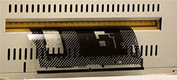

Stage 1 is to transfer the image using an artwork film to the board surface, using photosensitive dry-film and UV light, which will polymerise the dry film exposed by the artwork. This step of the process is performed in a clean room.<br> Imaging – The process of transferring electronic data to the photo-plotter, which in turn uses light to transfer a negative image circuitry pattern onto the panel or film.


Stage 2 is to remove the unwanted copper from the panel using etching. Once this copper has been removed, the remaining dry film is then removed leaving behind the copper circuitry that matches the design.<br> Etching – The chemical, or chemical and electrolytic, removal of unwanted portions of conductive or resistive material.

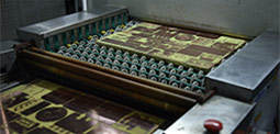

Inspection of the circuitry against digital “images” to verify that the circuitry matches the design and that it is free from defects. Achieved through scanning of the board and then trained inspectors will verify any anomalies that the scanning process has highlighted. PCBWay Group allows no repair of open circuits.
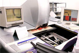

The inner layers have an oxide layer applied and then “stacked” together with pre-preg providing insulation between layers and copper foil is added to the top and bottom of the stack. The lamination process consists of placing the internal layers under extreme temperature (375 degrees Fahrenheit) and pressure (275 to 400 psi) while laminating with a photosensitive dry resist. The PCB is allowed to cure at a high temperature, the pressure is slowly released and then the material is slowly cooled.
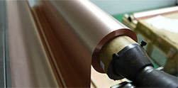
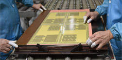

We now have to drill the holes that will subsequently create electrical connections within the multilayer PCB. This is a mechanical drilling process that must be optimised so that we can achieve registration to all of the the inner layer connections. The panels can be stacked at this process. The drilling can also be done by a laser drill
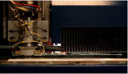

The first step in the plating process is the chemical deposition of a very thin layer of copper on the hole walls.
PTH provides a very thin deposit of copper that covers the hole wall and the complete panel. A complex chemical process that must be strictly controlled to allow a reliable deposit of copper to be plated even onto the non-metallic hole wall. Whilst not a sufficient amount of copper on its own, we now have electrical continuity between layers and through the holes.Panel plating follows on from PTH to provide a thicker deposit of copper on top of the PTH deposit – typically 5 to 8 um. The combination is used to optimise the amount of copper that is to be plated and etched in order to achieve the track and gap demands.
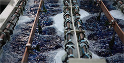
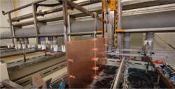

Similar to the inner layer process (image transfer using photosensitive dry film, exposure to UV light and etching), but with one main difference – we will remove the dry film where we want to keep the copper/define circuitry – so we can plate additional copper later in the process.
This step of the process is performed in a clean room.
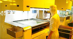

Second electrolytic plating stage, where the additional plating is deposited in areas without dry film (circuitry). Once the copper has been plated, tin is applied to protect the plated copper.
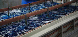
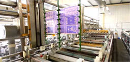

This is normally a three step process. The first step is to remove the blue dry film. The second step is to etch away the exposed/unwanted copper whilst the tin deposit acts an etch resist protecting the copper we need. The third and final step is to chemically remove the tin deposit leaving the circuitry.
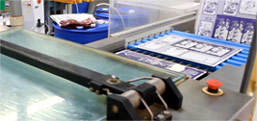
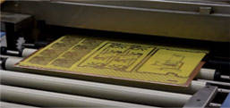

Just like with inner layer AOI the imaged and etched panel is scanned to make sure that the circuitry meets design and that it is free from defects. Again no repair of open circuits are allowed under PCBWay demands.
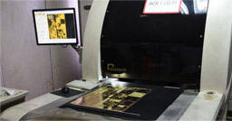

Soldermask ink is applied over the whole PCB surface. Using artworks and UV light we expose certain areas to the UV and those areas not exposed are removed during the chemical development process – typically the areas which are to be used as solderable surfaces. The remaining soldermask is then fully cured making it a resilient finish.<br> This step of the process is performed in a clean room.
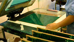

Various finishes are then applied to the exposed copper areas. This is to enable protection of the surface and good solderability. The various finishes can include Electroless Nickel Immersion Gold, HASL, Immersion Silver etc. Thicknesses and solderability tests are always carried out.
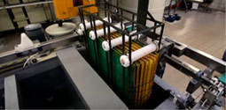
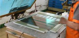

This is the process of cutting the manufac-turing panels into specific sizes and shapes based upon the customer design as defined within the gerber data. There are 3 main options available when providing the array or selling panel – scoring, routing or punching. All dimensions are measured against the customer supplied drawing to ensure the panel is dimensionally correct.
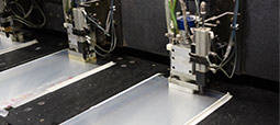
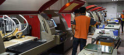

Used for checking the integrity of the tracks and the through hole interconnections – checking to ensure there are no open circuits or no short circuits on the finished board. There are three test methods, flying probe for smaller volumes,fixture based for volumes and 4-wire Kelvin testing (For PCBs use in automotive, or aerospace applications).We electrically test every PCB against the original board data. Using a flying probe tester we check each net to ensure that it is complete (no open circuits) and does not short to any other net.
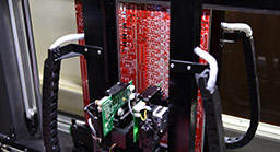

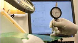
In the last step of the process a team of sharp-eyed inspectors give each PCB a final careful check-over.Visual checking the PCB against acceptance criteria and using PCBWay “approved” inspectors. Using manual visual inspection and AVI – compares PCB to gerber and has a faster checking speed that human eyes, but still requires human verification. All orders are also subjected to a full inspection including dimensional, solderability, etc.
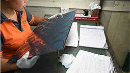

Boards are wrapped using materials that comply with the PCBWay Packaging demands (ESD etcetera) and then boxed prior to be being shipped using the requested mode of transport.
