PCB Prototype the Easy Way
Full feature custom PCB prototype service.
9:00 - 18:00, Mon.- Fri. (GMT+8)
9:00 - 12:00, Sat. (GMT+8)
(Except Chinese public holidays)
PCB Prototype the Easy Way
Full feature custom PCB prototype service.
9:00 - 18:00, Mon.- Fri. (GMT+8)
9:00 - 12:00, Sat. (GMT+8)
(Except Chinese public holidays)
PCBWay is a professional quick-turn PCB prototyping, PCB Assembly and low-volume production manufacturer located in Shenzhen China. (3 major PCBs and 2 PCB Assembly production).
The information below details some of the key capabilities that PCBWay can offer and support today. You will find information here relating to the specific materials we can support, the PCB technologies or product types that we currently produce, as well as some of the tolerances which we can achieve.
The first category is what we call "Quick-turn" which means we can offer Small Quantity - Quick Turn PCBs, Custom Spec - Standard PCBs, and Quick-order PCBs (Gerber Viewer).
The second is our “Advanced” offering and this shows the very best that PCBWay can offer: Full Spec PCBs, Highly Specialized Precision PCBs, & Large Scale Production, but sometimes some plates and materials are temporarily out of stock.
Please send messages to your sales rep if your boards are beyond the capabilities listed below.
“Standard PCB” = Advanced + quick-order
| Items | Manufacturing Capabilities | Remarks | |
|---|---|---|---|
| Number of Layers | - | 1-10 layers | For orders above 10 layers,please view the below "Standard PCB" or contact our sales rep. |
| Material | - |
FR-4,Aluminum
|
For Flex, Rigid-flex, Metal-based (Aluminum etc.,), HDI, Halogen-free, High Tg, etc.,please view the below "Standard PCB" or contact sales rep. |
| Maximum PCB Size(Dimension) | - | 500*1100mm (min 5*6mm) | Any sizes beyond this dimension, please view the below "Standard PCB" or contact sales rep. |
| Board Size Tolerance(Outline) | - | ±0.2mm/±0.5mm | ±0.2mm for CNC routing, and ±0.5mm for V-scoring. |
| Board Thickness |  |
0.2-2.4mm | 0.2,0.4, 0.6, 0.8, 1.0, 1.2, 1.6, 2.0, 2.4mm. Please view the below "Standard PCB" or contact us if your board exceeds these. |
| Board Thickness Tolerance(t≥1.0mm) | - | ±10% | Normally “+ Tolerance” will occur due to PCB processing steps such as electroless copper, solder mask and other types of finish on the surface. |
| Board Thickness Tolerance(t<1.0mm) | - | ±0.1mm | |
| Min Trace |  |
0.1mm/4mil | Min manufacturable trace is 4mil(0.1mm), strongly suggest to design trace above 6mil(0.15mm) to save cost. |
| Min Spacing | Min manufacturable spacing is 4mil(0.1mm), strongly suggest to design spacing above 6mil(0.15mm) to save cost. | ||
| Outer Layer Copper Thickness |  |
1oz/2oz/3oz(35μm/70μm/105μm) | Also known as copper weight. 35μm=1oz, 70μm=2oz, 105μm=3oz. Please view the below "Standard PCB" or contact us if you need copper weight greater than 3oz. |
| Inner Layer Copper Thickness |  |
1oz/1.5oz(35μm/50μm) | Inner copper weight as per customer’s request for 4 and 6 layers(Multi-layer laminated structure). Please contact us if you need copper weight greater than 1.5oz. |
| Drill Sizes (CNC) |  |
0.2-6.3mm | Min drill size is 0.2mm, max drill is 6.3mm. Any holes greater than 6.3mm or smaller than 0.3mm will be subject to extra charges. |
| Min Width of Annular Ring |  |
0.15mm(6mil) | For pads with vias in the middle, Min width for Annular Ring is 0.15mm(6mil). |
| Finished Hole Diameter (CNC) |  |
0.2mm-6.2mm | The finished hole diameter will be smaller than size of drill bits because of copper plating in the hole barrels |
| Finished Hole Size Tolerance(CNC) | - | ±0.08mm | For example, if the drill size is 0.6mm, the finished hole diameter ranges from 0.52mm to 0.68mm will be considered acceptable. |
| Solder Mask |  |
LPI | Liquid Photo-Imageable is the mostly adopted. Thermosetting Ink is used in the inexpensive paper-based boards. |
| Minimum Character Width(Legend) |  |
0.15mm | Characters of less than 0.15mm wide will be too narrow to be identifiable. |
| Minimum Character Height (Legend) | - | 0.8mm | Characters of less than 0.8mm high will be too small to be recognizable. |
| Character Width to Height Ratio (Legend) | - | 1:5 | In PCB silkscreen legends processing, 1:5 is the most suitable ratio |
| Minimum Diameter of Plated Half Holes | - | 0.6mm | Design Half-Holes greater than 0.6mm to ensure better connection between boards. |
| Surface Finishing |  |
HASL with lead HASL lead free Immersion gold,OSP |
The most popular three types of PCB surface finish. Please view the below "Standard PCB" or contact us for other finishes. |
| Solder Mask |  |
Green ,Red, Yellow, Blue, White ,Black |
No extra charge (Green, Red, Yellow, Blue) |
| Silkscreen |  |
White, Black, None |
No extra charge. |
| Panelization |  |
V-scoring, Tab-routing, Tab-routing with Perforation (Stamp Holes) |
Leave min clearance of 1.6mm between boards for break-routing. For V-score panelization, set the space between boards to be zero. |
| Others | - | Fly Probe Testing (Free) and A.O.I. testing(free), ISO 9001:2008 ,UL Certificate |
No extra charge. |
| Categories | No. | Items | PCB process parameters | Remarks | |||||
|---|---|---|---|---|---|---|---|---|---|
| Normal process | Medium difficulty | High difficulty | |||||||
| Non-standard review | Unable to make | ||||||||
| product type | 1 | Multilayer PCB Layers | 3L≤Layers≤16L | 18L≤Layers≤24L | ≥24L | ||||
| 2 | Blind and Buried Vias | HDI(1+1+....+N+......+1+1) | Anylayer HDI | HDI(2+...+N...+2) | If meet the requirements of 2, 6, and 21 at the same time, it is classified as a high requirement product (thickness to diameter ratio, copper thickness of hole) | ||||
| 3 | Surface Coating | HASL(+gold finger),immersion gold, Immersion Gold +gold fingers with hard gold,OSP (+gold finger with hard gold), Immersion Tin (+gold finger with hard gold) (Not two different surface finish),Immersion Tin | Local immersion gold (long or short gold fingers, segmented gold finger craft) | Exceed this range require unconventional production processes | Partial immersion gold, thickness of gold or nickel reference to the thickness of the coating | ||||
| 4 | Board Material | FR-4;aluminum,Rogers4 series + FR-4 mixed(The Prepreg is ShengYi brand and ROGERS4403 series);CEM-3、LianMao IT158/IT180A | Pure ROGERS4 series multi-layer board (Prepreg is 4450F),PTFE、aluminum+FR4、PTFE+FR4 | Exceed this range require unconventional production processes | Pure PTFE multi-layer board | Pure PTFE can’t be made because the lamination temperature isn’t up to standard,Can‘t laminate Rogers copper foil directly | |||
| Drills | 5 | Drill diameter | Nc drill | 0.20mm≤Drill diameter≤6.5mm More than 6.0mm using CNC milling hole diameter 0.2mm: maximum board thickness 1.6mm hole diameter diameter 0.25mm:maximum board thickness 2.0mm, hole diameter 0.3mm≤Ф≤0.35mm, maximum board thickness 3.2 mm, hole diameter 0.4mm≤Ф≤0.55mm, maximum board thickness 4.8 mm, hole diameter>0.55mm maximum board thickness 6.4 mm |
6.5mm or more ±0.1mm ≤ hole diameter tolerance (using CNC milling for 6.5mm or more) | The drill diameter more than 6.0mm, the hole diameter tolerance less than ±0.1mm. If exceed this range require unconventional production processes | Drill diameter below 0.2mm, and the aspect ratio≥10, which is medium difficulty | ||
| 6 | Thickness to diameter ratio | Thickness to diameter ratio≤8 | 8| 10 | Thickness to diameter ratio greater than 12 when the aperture cannot be compensated |
If need to meet the requirement of 2, 6, and 21, it will be treat as high requirement product. |
| |||
| 7 | countersink | hole diameter | 3.0mm≤hole diameter≤6.5mm | Unconventional production beyond this range | Countersink depth tolerance is controlled 0.15mm | ||||
| Angle | 90° | Unconventional production beyond this range | |||||||
| 8 | Hole position tolerances | ±0.075mm | ±0.05mm | <+/-0.05mm | |||||
| 9 | hole diameter tolerance | PTH | ±0.075mm or no customer requirements | ±0.05≤ hole diameter tolerance <±0.75mm | <±0.05mm | <+/-0.05mm | Metallized hole diameter tolerance of 6.0mm or more refers to the requirement of serial number 5 | ||
| NPTH | ≥±0.075mm | <±0.05mm | <+/-0.025mm | ||||||
| Special hole | pressfit | ≤±0.05 | \ | \ | |||||
| non-plated Countersink/Counterbore holes(NPTH) | hole diameter <10mm:tolerance ±0.15mm,hole diameter ≥10mm:tolerance ± 0.20mm | \ | \ | ||||||
| non-plated Countersink/Counterbore holes(NPTH) | hole diameter <10mm:tolerance ±0.2mm hole diameter ≥10mm:tolerance+0.3mm |
\ | \ | ||||||
| 10 | Hole to hole spacing | component hole | ≥16MIL | 14≤Hole to hole spacing≤16 | 13≤Hole to hole spacing≤14 | <13mil | |||
| via(≤0.45mm) | ≥11MIL | ||||||||
| 11 | Slot (Cut-out) | Slot width | Plated slot ≥0.5mm Non-plated slot ≥0.8mm |
\ | \ | More than 1.0mm, can be slot by machine | |||
| Length to width ratio of slot | Length to width≥2 | Length to width<2 | |||||||
| 12 | Castellated Holes | Castellated Holes diameter | ≥0.5mm | 0.5mm>diameter≥0.4mm | \ | ||||
| Castellated Holes spacing (edge to edge) | ≥0.3mm | 0.3mm>diameters≥0.2mm | \ | ||||||
| 13 | Minimum isolation ring of Inner layer, The distance between minimum hole in Inner layer and circuit (before compensation) |
4L | ≥7MIL | 6MIL≤isolation ring, distance<7MIL | 5MIL≤isolation ring, distance<6MIL | If the size of one side is greater than 600MM, the inner hole to line and the hole to copper spacing must be greater than or equal to 15mil. If less than 15mil, it must be treated as unconventional review. The conventional process of 10 layers or more need to be incremented by 1 mil for each additional 2 layers. Change the isolation ring to 12mil or more as much as possible | |||
| 6L | ≥8MIL | 6.5MIL≤isolation ring, distance<8MIL | 6MIL≤isolation ring, distance<6.5MIL | ||||||
| 8L | ≥9MIL | 7MIL≤isolation ring, distance<9MIL | 6MIL≤isolation ring, distance<7MIL | ||||||
| ≥10L | ≥10MIL | 8MIL≤isolation ring, distance<10MIL<9MIL | 7MIL≤isolation ring, distance<8MIL | ||||||
| image transfer | 14 | The min width/spacing of inner layer (before compensation) | copper thickness 18um | ≥4/4 mil | ≥4/3.5 mil | <3.5/3 mil | width/spacing | ||
| copper thickness 35um | ≥4/5 mil | ≥4/4 mil | <3.5/4 mil | width/spacing | |||||
| copper thickness 70um | ≥6/8mil | ≥6/7mil | <5/6 mil | width/spacing | |||||
| copper thickness 105um | ≥8/11 mil | ≥8/10 mil | <6/9 mil | width/spacing | |||||
| 15 | The min width/spacing of outer layer (before compensation) | copper thickness 18um | ≥4/5 mil | ≥4/4 mil or parts 3.5/3.5mil | <3.5/3.5 mil | Local 3.5/3.5mil, only the distance from the GBA chip area line to the PAD | |||
| copper thickness 35um | ≥5/6 mil | ≥5/5 mil | <4/4 mil | ||||||
| copper thickness 70um | ≥7/8mil | ≥6/7mil | <5/6 mil | ||||||
| copper thickness 105um | ≥10/12 mil | ≥8/10 mil | <6/9 mil | ||||||
| 16 | grid trace width/spacing | copper thickness 18um | ≥7/9 mil | ≥6/8 mil | <6/7 mil | ||||
| copper thickness 35um | ≥9/11 mil | ≥8/10 mil | <8/9 mil | ||||||
| copper thickness 70um | ≥11/13mil | ≥10/12mil | <10/11 mil | ||||||
| copper thickness 105um | ≥13/15 mil | ≥12/14 mil | <12/13 mil | ||||||
| 17 | Minimum weld ring (outer layer) | copper thickness 18um | via hole | ≥5mil | ≥4mil | <3 mil | |||
| component hole | ≥8mil | ≥6mil | <6 mil | ||||||
| copper thickness 35um | via hole | ≥5mil | ≥4mil | <3 mil | |||||
| component hole | ≥10mil | ≥8mil | <8 mil | ||||||
| copper thickness 70um | via hole | ≥7mil | ≥6mil | <5 mil | |||||
| component hole | ≥12mil | ≥10mil | <10 mil | ||||||
| copper thickness 105um | via hole | ≥8mil | ≥6mil | <6 mil | |||||
| component hole | ≥14mil | ≥12mil | <12 mil | ||||||
| 18 | width tolerance | width tolerance:≥±20% | ±10%≤ width tolerance:<±20% | <±10% | spacing must meet the requirements of 11 and 12, lf width is greater than 15mil, controlled by ±2.5mil | ||||
| BGA pad diameter | hot air leveling (original) | ≥12MIL | ≥10MIL | <8mil | |||||
| immersion gold (original) | diameter≥11mil | 8.0mil≤diameter<11.0mil | <6mil | ||||||
| 19 | Line to board edge distance | CNC milling | 0.25mm | 0.20mm | <0.20mm | ||||
| SMT width | ≥12mil | ≥9mil | <9mil以下 | <7mil,except the binding board | |||||
| Metal plating | 20 | Plating Thickness(µin) | Electroless Nickel-Immersion Gold,ENIG | Nickel thickness | 100-150 µin | 200 µin | |||
| gold thickness | 1-8 µin | >8 µin | |||||||
| Full board gold plating | Nickel thickness | 100-150 µin | 200-500 µin | Order center check the final price | |||||
| gold thickness | 1-10 µin | 10-50 µin | >50 µin | ||||||
| gold finger | Nickel thickness | 120-150 µin | 200-400 µin | ||||||
| gold thickness | 1-30 µin | 30-50 µin | >50 µin | ||||||
| 21 | Hole copper thickness (µm) | Through hole | 18-25 µm | 30-50 µm | >50 µm | If 2,6,19 is required to exist at the same time, it will be treated as high requirement. The thickness of the copper is 25-50UM, and the thickness of the copper is required to be 2-3OZ generally. | |||
| Blind hole (mechanical hole) | 18-25 µm | 30-50 µm | >50 µm | ||||||
| Buried hole | 15-25 µm | 30-50 µm | >50 µm | ||||||
| 22 | Bottom copper thickness | Inner and outer copper thickness (OZ) | 0.5-4 | 4-6 | >6 | ||||
| solder mask | 23 | solder mask | green solder mask opening(mil) | ≥2mil | 1.5 | 1 | 1mil is only concentrated in the BGA area. If the window can be enlarged, increase it as much as possible, but the maximum is 3mil | ||
| green solder mask Bridge(mil) | copper thicknesss<2OZ | 4(spacing between ICs is 8 mil, green oil),variegated or black oil≥4.5mil | 3-4(spacing between ICs is 7-8 mil, green oil),variegated or black oil≥4mil | ||||||
| copper thicknesss≥2OZ | 5 | 4 | |||||||
| Plug Hole diameter | 0.20mm≤hole diameter≤0.40mm,plug hole fullness 70% | 0.4mm< hole diameter ≤0.70mm | fullness 100% | ||||||
| Plug Hole board thickness | 0.40mm≤board thickness≤2.4mm | >2.4MM | |||||||
| 24 | solder mask | solder mask color | Green, matt green, blue, red, black, matte black, white, yellow | \ | \ | Special colors need to be purchased or deployed in advance | |||
| silkscreen | 25 | Etched silkscreen (finished copper thickness) | Copper thickness 18um | word width/word height | 8MIL/40MIL | 7MIL/35MIL | |||
| Copper thickness 35um | word width/word height | 9MIL/40MIL | 8MIL/35MIL | ||||||
| Copper thickness 75um | word width/word height | 12MIL/60MIL | 10MIL/50MIL | ||||||
| Copper thickness 105um | word width/word height | 16MIL/60MIL | 14MIL/50MIL | ||||||
| outline | 26 | Maximum board thickness | Double PCB | 3.2MM | 4.5MM | >4.5MM | calculated by 4 layers if the thickness more than 3mm | ||
| Multilayer layer board | 3.2MM | 4.5MM | >4.5MM | ||||||
| 27 | Minimum board thickness (single and double panel refers to substrate thickness) | Single or Double side PCB (pcb prototype) | ≥0.3mm | 0.25mm | |||||
| 4L | ≥0.60mm | 0.40mm | <0.40mm | ||||||
| 6L | ≥0.9mm | 0.70mm | <0.70mm | ||||||
| 8L | ≥1.20mm | 1.00mm | <1.00mm | ||||||
| 10L | ≥1.40mm | 1.20mm | <1.20mm | ||||||
| 12L | ≥1.70mm | 1.50mm | <1.50mm | ||||||
| 14L | ≥2.00mm | 1.80mm | <1.80mm | ||||||
| 28 | thickness (T) tolerance MM (multilayer layer pcb) | T≤1.0 | ±0.10 | Need to review if less than the tolerance | If the tolerance is unilateral tolerance, the tolerance shall be double tolerance value, such as: 1.8mm requires positive tolerance, the tolerance shall be 0-0.36mm | ||||
1.0| ±0.13 |
| | |||||||
1.6| ±0.18 |
| | |||||||
2.5| ±0.23 |
| | |||||||
| T≥3.2 | ±8% | ||||||||
| 29 | Maximum finished board size | Single and double side PCB | 508×610mm | Beyond this range needs to be reviewed | |||||
| Multilayer Layer PCB | 508×600mm | ||||||||
| 30 | Minimum finished pcb size | ≥20mm | 10mm≤Size<20mm | <10mm | |||||
| 31 | Beveling for gold finger | Bevel angle | 20°30°45°60° | <20°Or>60° | |||||
| Bevel angle tolerance | >±5° | ±5° | <±5° | ||||||
| Bevel depth tolerance | tolerance≥±0.15mm | ±0.15mm< Tolerance ≤ ±0.1mm | tolerance<±0.10mm | ||||||
| 32 | Shape tolerance | tolerance≥±0.15mm | ±0.10mm≤tolerance<±0.15mm | Tolerance<±0.10mm or more than two form tolerance control | |||||
| 33 | V-CUT | Angle | 20°30°45°60° | ||||||
| The Maximum number of V-CUT | In 20 times | In 30 times | In 40 times | ||||||
| Width of the shape | 80MM< width <560MM | 60MM< width <80MM | width <60MM | ||||||
| board thickness | 0.6MM≦thickness≦2.4MM | 0.5MM≦thickness<0.6MM | thickness<0.5MM or thickness>2.4MM | below 0.5mm is single-sided V-CUT | |||||
| Remaining thickness | ≥0.25MM | <0.25MM | |||||||
| V-CUT | Conventional V-CUTT、V-CUT: Skip V-CUT | \ | \ | ||||||
| others | 34 | panel size | The minimum panel size | ≥100*120mm | \ | <100*120mm | The thickness of the finished board is less than 0.4MM, the panel size can’t exceed 14inch, and the maximum size of the HASL PCB can’t exceed 24inch | ||
| the Maximum panel size | ≤20*24 inch | \ | Need to review if beyond range | ||||||
| 35 | impedance control | Impedance control tolerance | ±10%,50Ω and below:±5Ω | \ | <±10%,50Ω and below <±5Ω | ||||
| bow and twist | bow and twist tolerance | bow and twist≤0.75% | 0.5%≤bow and twist≤ 0.75% | bow and twist<0.5% | asymmetry boards bow and twist tolerance 1.2% | ||||
| 36 | HASL processing capacity | component hole diameter | hole diameter>0.5mm | 0.4mm≤hole diameter≤0.5mm | |||||
| board thickness | 0.5mm≤board thickness≤3.5mm | 0.4mm≤board thickness<0.5mm | |||||||
| thickness | 2um≤thickness of Tin≤30um | \ | \ | ||||||
| 37 | Acceptance Criteria | IPC standard | IPC2 level standard | IPC Level 3 standard | |||||
Thanks for reviewing our PCB capabilities. Please upload your PCB files in the format of gerber file, .pcb, .pcbdoc or .cam file when you go through our online purchase procedures. Please try best to offer gerber file. But if you only have DXP file with (.pcb/.pcbdoc) format, we will use ALtium Designer23.21 and 10.0 software to transfer to gerber.So please avoid higher version than AD 23.21 and 10.0 .You can also send your Gerber to your sales rep, but we strongly suggest you order online on the webpages.


 Smart Devices: We have large customer base in these industries. Customers choose us to make their PCBs in the prototype and production stage.
 Medicine: Medicine and biomedical clients occupy a large part of our customers. We have strict quality standard and short lead time and our price is competitive, our customer base in this area is still on the rise.
 Commercial, industrial and automotive:
Most of our customers are in these industries. Fast response, short delivery time, professional engineering support continuously affordable price help retain and expand customer scale in these industries.
 University, school and amateur:
Students are our future scientists, we support them! Students and amateurs are price sensitive customers, our price guarantees they will rely on us for their PCB needs in terms of price and quality! At the same time, our educational sponsorship program provides free PCBs to university students, please send us the details of your project or competition at service@pcbway.com.
Contact Us!
Our customer service+86-571-85317532
 I am impressed with the quality of the boards, the delivery time and responce to all my questions. Best price excellent service and speedy delivery. When I need another board I will certainly use this supplier. "
 спасибо за платы! платы очень хорошего качества. надежный продавец. оперативно отвечал на вопросы. заказ выполнили и отправили очень быстро.Заказываю платы не в первый раз - как всегда только лучшие впечатления. 5+++. 4 числа отправил файлы 26-го забрал на почте в Москве."

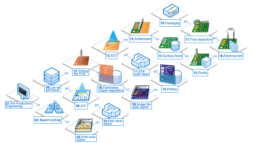
Customer supplied data (gerber) is used to produce the manufacturing data for the specific PCB (artworks for imaging processes and drill data for drilling programs). Engineers compare demands/specifications against capabilities to ensure compliance and also determine the process steps and associated checks. No changes are allowed without PCBWay Group permission.



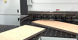
PCB production starts with a large piece of sheet material. Due to the limitations of PCB production equipment and manufacture capabilities, the factory has requirements for its minimum and maximum processing size. Therefore, under the guidance of manufacture instruction (MI), the raw material of PCB (Copper Clad Laminate ) needs to be cut into the processing size by automatic cutting machine before production.

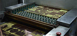
Stage 1 is to transfer the image using an artwork film to the board surface, using photosensitive dry-film and UV light, which will polymerise the dry film exposed by the artwork.
This step of the process is performed in a clean room.
Imaging – The process of transferring electronic data to the photo-plotter, which in turn uses light to transfer a negative image circuitry pattern onto the panel or film.


Stage 2 is to remove the unwanted copper from the panel using etching. Once this copper has been removed, the remaining dry film is then removed leaving behind the copper circuitry that matches the design.
Etching – The chemical, or chemical and electrolytic, removal of unwanted portions of conductive or resistive material.


Inspection of the circuitry against digital “images” to verify that the circuitry matches the design and that it is free from defects. Achieved through scanning of the board and then trained inspectors will verify any anomalies that the scanning process has highlighted. PCBWay Group allows no repair of open circuits.


The inner layers have an oxide layer applied and then “stacked” together with pre-preg providing insulation between layers and copper foil is added to the top and bottom of the stack. The lamination process consists of placing the internal layers under extreme temperature (375 degrees Fahrenheit) and pressure (275 to 400 psi) while laminating with a photosensitive dry resist. The PCB is allowed to cure at a high temperature, the pressure is slowly released and then the material is slowly cooled.



We now have to drill the holes that will subsequently create electrical connections within the multilayer PCB. This is a mechanical drilling process that must be optimised so that we can achieve registration to all of the the inner layer connections. The panels can be stacked at this process. The drilling can also be done by a laser drill


The first step in the plating process is the chemical deposition of a very thin layer of copper on the hole walls.
PTH provides a very thin deposit of copper that covers the hole wall and the complete panel. A complex chemical process that must be strictly controlled to allow a reliable deposit of copper to be plated even onto the non-metallic hole wall. Whilst not a sufficient amount of copper on its own, we now have electrical continuity between layers and through the holes.Panel plating follows on from PTH to provide a thicker deposit of copper on top of the PTH deposit – typically 5 to 8 um. The combination is used to optimise the amount of copper that is to be plated and etched in order to achieve the track and gap demands.



Similar to the inner layer process (image transfer using photosensitive dry film, exposure to UV light and etching), but with one main difference – we will remove the dry film where we want to keep the copper/define circuitry – so we can plate additional copper later in the process.
This step of the process is performed in a clean room.


Second electrolytic plating stage, where the additional plating is deposited in areas without dry film (circuitry). Once the copper has been plated, tin is applied to protect the plated copper.
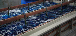


This is normally a three step process. The first step is to remove the blue dry film. The second step is to etch away the exposed/unwanted copper whilst the tin deposit acts an etch resist protecting the copper we need. The third and final step is to chemically remove the tin deposit leaving the circuitry.



Just like with inner layer AOI the imaged and etched panel is scanned to make sure that the circuitry meets design and that it is free from defects. Again no repair of open circuits are allowed under PCBWay demands.


Soldermask ink is applied over the whole PCB surface. Using artworks and UV light we expose certain areas to the UV and those areas not exposed are removed during the chemical development process – typically the areas which are to be used as solderable surfaces. The remaining soldermask is then fully cured making it a resilient finish.
This step of the process is performed in a clean room.
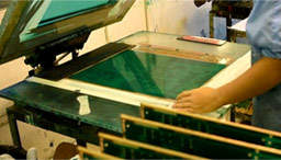

Various finishes are then applied to the exposed copper areas. This is to enable protection of the surface and good solderability. The various finishes can include Electroless Nickel Immersion Gold, HASL, Immersion Silver etc. Thicknesses and solderability tests are always carried out.

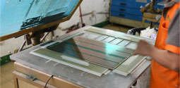

This is the process of cutting the manufac-turing panels into specific sizes and shapes based upon the customer design as defined within the gerber data. There are 3 main options available when providing the array or selling panel – scoring, routing or punching. All dimensions are measured against the customer supplied drawing to ensure the panel is dimensionally correct.



Used for checking the integrity of the tracks and the through hole interconnections – checking to ensure there are no open circuits or no short circuits on the finished board. There are three test methods, flying probe for smaller volumes,fixture based for volumes and 4-wire Kelvin testing (For PCBs use in automotive, or aerospace applications).We electrically test every PCB against the original board data. Using a flying probe tester we check each net to ensure that it is complete (no open circuits) and does not short to any other net.


In the last step of the process a team of sharp-eyed inspectors give each PCB a final careful check-over.Visual checking the PCB against acceptance criteria and using PCBWay “approved” inspectors. Using manual visual inspection and AVI – compares PCB to gerber and has a faster checking speed that human eyes, but still requires human verification. All orders are also subjected to a full inspection including dimensional, solderability, etc.
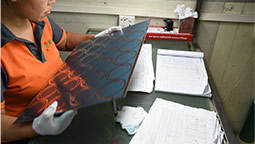


Boards are wrapped using materials that comply with the PCBWay Packaging demands (ESD etcetera) and then boxed prior to be being shipped using the requested mode of transport.
