Surface Mount Assembly Process
Originally, all PCBs were assembled by hand using only a solder iron. As technology progresses, components get smaller and more difficult to assemble by hand and the amount of components that may fit on a single board increases. Thus the need for auto assembly was developed.

Required Elements
The following are the required elements for auto assembly:
-
Gerbers in 274-X (embedded apertures) including fabrication drawing.
-
Part centroid text file with Reference Designators, external placement layer, and X & Y location and rotation in ASCII format.
-
Numerical control (NC) drill files
-
Solder paste file (one of the Gerber files) for all sides mounted
-
Glue dot file
-
If possible, the design database, specifying the database format (program name)
-
Parts list or BOM (bill of material)
-
Parts or hardware required
The Gerber files are used to define the pad locations and help the assembly house determine where pin 1 is located and provides a heads-up of how the board looks. The database can also be used to determine the location of pin 1. Some board houses choose to make their own solder paste file/stencil. The designer may create the solder paste file to his/her own preference with experience. It is good to learn how and why the assembly house makes its stencils and duplicate it to ensure consistency from each assembly house (the common name for any company that assembles boards). The solder paste file is used to mask the entire board except those areas that will be soldered. Solder paste is applied to the exposed pads and the stencil is removed. Components are applied and held to the board by the solder paste and the glue dots securing the components as they are soldered to the board.
For component placement a part placement/centroid file is required to know where the center of the part is. The layer ID shows what side the part is placed on, and the rotation displays the orientation of the component.
Consistency in rotation of the original component is critical to report. Unless the designer's software can account for inconsistencies, all components should be created in the same orientation.
NC drill files are used to locate mounting holes and provide the holes sizes for thru-hole components. This also allows the assembly house to determine adequate clearance for the component lead.
A bill of material or parts list is used to reference the designators of the centroid file and the components that need to be mounted. The BOM should also provide information if the component is an SM component or a thru-hole component.
Other Considerations
Other considerations for auto assembly are the board size, the panel size, and breakaways. The boards are commonly assembled in a panel that may contain many boards. The panel is the original material that the boards were etched routed in. The panels pass to the assembly house with all boards intact.
Note
Breakaways are the connections around a board that hold the board during assembly but can be broken easily when it is time to remove the board.
1.Ordering a Board
PCBWay One-Stop Solution for PCB & Prototype Assembly,
2.DFM Check
The DFM check looks at all the design specifications of a PCB. Specifically, this check looks for any missing, redundant or potentially problematic features. Any of these issues may severely and negatively influence the functionality of the final project. For example, one common PCB design flaw is leaving too little spacing between PCB components. This can result in shorts and other malfunctions.
By identifying potential problems before manufacturing begins, DFM checks can cut manufacturing costs and eliminate unforeseen expenses. This is because these checks cut down on the number of scrapped boards. As part of our commitment to quality at a low cost.

3.Incoming Quality Control(IQC)
PCBWay Verifying all incoming materials and handling quality problems before subsequent SMT assembly begins. Our IQC position will check following issues of incoming materials if they comply with our strict requirements.
• model number and quantities according to BOM list
• shape (deformation, broken pin, oxidation etc), particularly for IC or other complex components
• sample test of incoming materials by tools such as test frame, multimeter etc.
• If above defect or discrepancy occurs, we will return full incoming materials to supplier or customer.
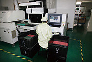
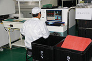
4.Machine programming - Gerber / CAD to Centroid / Placement / XY file
Having received the PCB panels and components the next step is to setup the various machines used with the manufacturing process. Machines such as the placement machine and AOI (Automated Optical Inspection) will require a program to be created which is best generated from CAD data but quite often this isn't available. Gerber data is almost always available as this is the data required for the bare PCB to be manufactured.
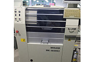
5.Solder Paste Printing
The first machine to setup in the manufacturing process is the solder paste printer which is designed to apply solder paste using a stencil and squeegees to the appropriate pads on the PCB.

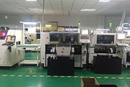
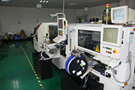
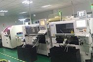
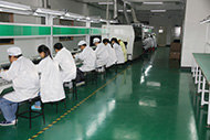
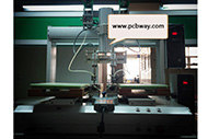
6.Component Placement
Once the printed PCB has been confirmed to have the correct amount of solder paste applied it moves into the next part of the manufacturing process which is component placement. Each component is picked from its packaging using either a vacuum or gripper nozzle, checked by the vision system and placed in the programed location at high speed.
There is a large variety of machines available for this process and it depends greatly on the business to what type of machine is selected. For example if the business is focused around large build quantities then the placement rate will be important however if the focus is small batch/high mix then flexibility will be more important.

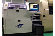
7.Pre-Reflow Automated Optical Inspection (AOI)
Following the component placement process it is important to verify that no mistakes have been made and that all parts have been correctly placed before reflow soldering. The best way of doing this is by using an AOI machine to make checks such as component presence, type/value and polarity.

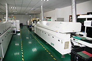
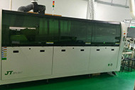
8.Reflow Soldering
Once the components are placed on the boards, each piece is sent through our reflow machines. This means the solder paste needs to solidify, adhering components to the board. PCB assembly accomplishes this through a process called "reflow".
This would appear to be one of the less complicated parts of the assembly processes but the correct reflow profile is key to ensure acceptable solder joints without damaging the parts or assembly due to excessive heat.
When using lead-free solder a carefully profiled assembly is even more important as the required reflow temperature can often be very close to many components maximum rated temperature.

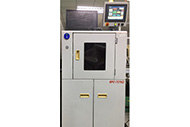
9.Post-Reflow Automated Optical Inspection (AOI)
The last part of the surface mount assembly process is to again check that no mistakes have been made by using an AOI machine to check solder joint quality.
Often, movement during the reflow process will result in poor connection quality or a complete lack of a connection. Shorts are also a common side effect of this movement, as misplaced components can sometimes connect portions of the circuit that should not connect.
Checking for these errors and misalignments can involve one of several different inspection methods. The most common of these inspection methods include the following:
- Manual Checks
- Automatic Optical Inspection(AOI)
- Automated X-ray inspection(AXI)

10.Conformal Coating
Some completed Printed Circuit Board Assemblies have a conformal coating. It's usually depends on the customer's product requirements.
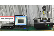
11.Final Inspection and Functional Test
After the soldering and conformal coating step of the PCB assembly process is finished, a final inspection will test the PCB for its functionality by our Quality Assurance team. This inspection is known as a "functional test". The test software and tools are usually provided by the customer, PCBWay can also make fixtures according to customer requirements. The test puts the PCB through its paces, simulating the normal circumstances in which the PCB will operate. Power and simulated signals run through the PCB in this test while testers monitor the PCB's electrical characteristics.
12.Washing and Drying
Suffice it to say, the manufacturing process can be a filthy one. Soldering paste leaves behind some amount of flux, while human handling can transfer oils and dirt from fingers and clothing to the surface of the board. Once all is said and done, the results can look a little dingy, which is both an aesthetic and a practical issue.
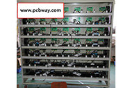
13.Packing and Shipping

All assembled boards are packaged (can request in anti-static packaging) and shipped DHL,FedEx,UPS,EMS,and so on. Any unused components are returned in accordance with customer instructions. Additionally, customers are notified via email when their packages ships.


 I am impressed with the quality of the boards, the delivery time and responce to all my questions. Best price excellent service and speedy delivery. When I need another board I will certainly use this supplier. "


